×
模态框(Modal)标题
在这里添加一些文本
Close
Close
Submit
Cancel
Confirm
×
模态框(Modal)标题
×
Journal
Article
Figure
Search
EN
中文
Home
About Journal
About Journal
Indexed in
Awards
Editorial Board
Guide for Authors
Browse
Current Issue
Online First
Archive
Highlights
Topic
Archive by Subject
Most Viewed
Most Download
Most Cited
E-mail Alert
RSS
Subscribe
Advertisement
Contact us
EN
中文
Figure/Table detail
Spatial Agglomeration Identification and Agglomeration Zoning of Semiconductor Industry in China
JIANG Xiaorong, LIU Qing
Economic geograph
, 2024, 44(
3
): 108-117. DOI:
10.15957/j.cnki.jjdl.2024.03.011
企业类型
芯片设计
晶圆材料
封测材料
封装测试
半导体制造
终端设备生产
总量
半导体企业数量(家)
3837
1767
2165
1841
3020
3127
15757
投资分支企业数量(家)
2141
2022
1300
1526
1671
1406
10066
Tab.1
Data on Chinese semiconductor enterprises and their investment branches
Other figure/table from this article
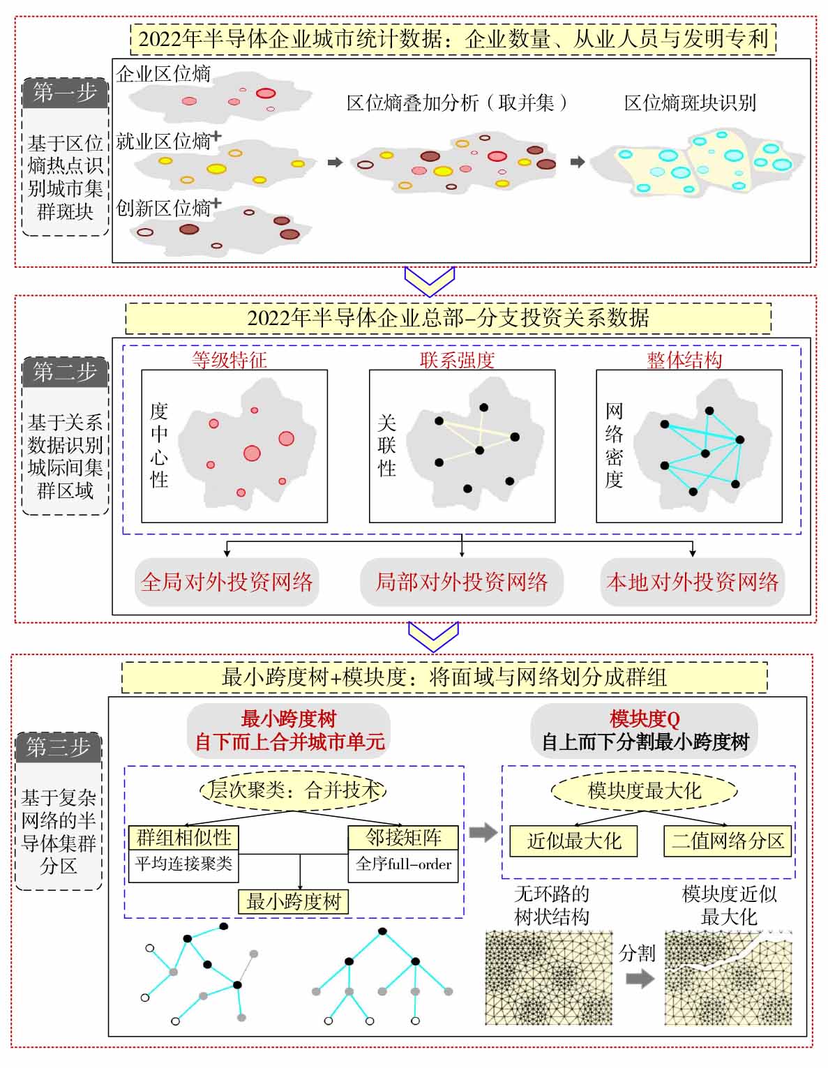
Fig.1
Framework and technological roadmap of agglomeration zone of China’s semiconductor industry
Fig.2
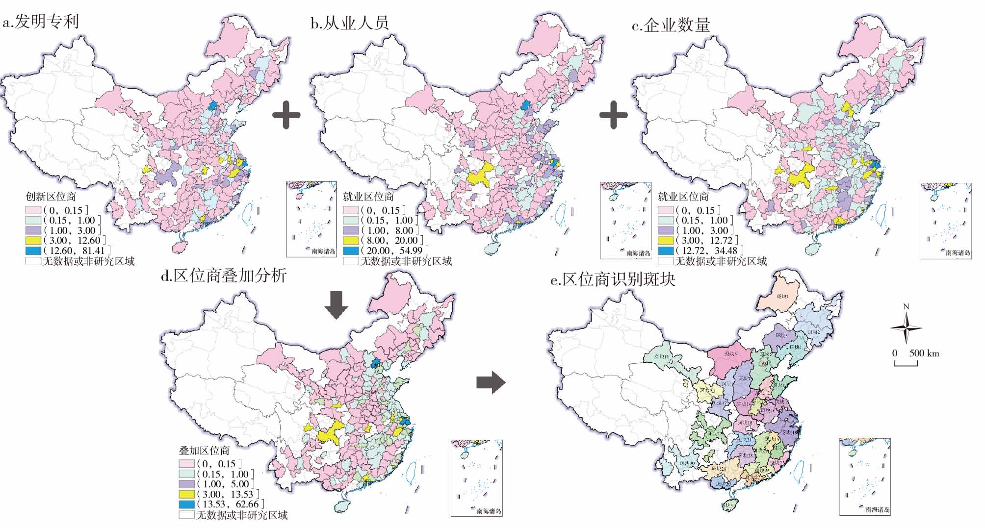
Hotspot identification of China semiconductor industry based on the locational quotient
Fig.3
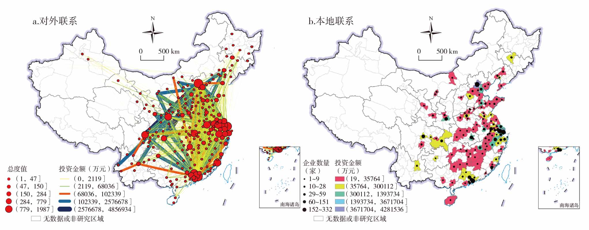
Overall network pattern of China’s semiconductor industry agglomeration based on outward and local investment of semiconductor enterprises
Fig.4
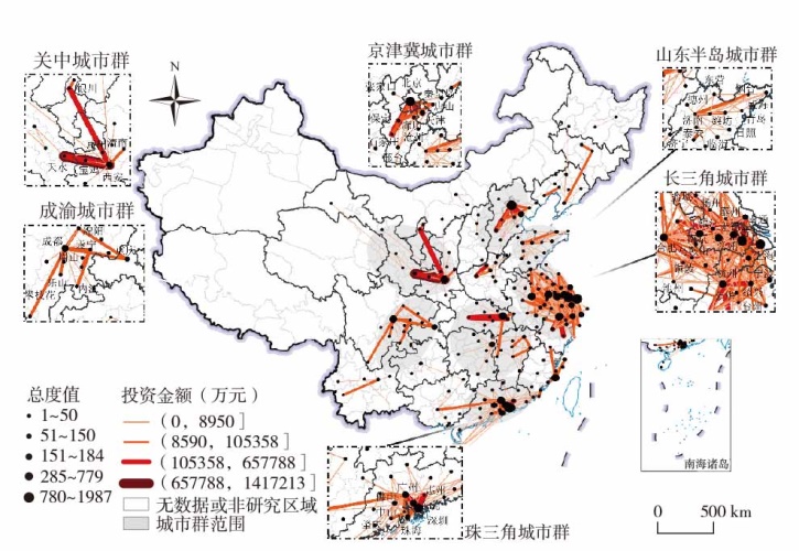
Regional network of China’s semiconductor industry agglomeration based on investment linkages of semiconductor enterprises
Fig.5
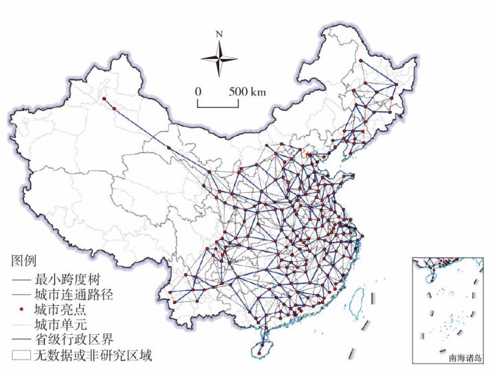
Pathway distribution of minimum weight spanning tree based on the spatial contiguity graph
Fig.6
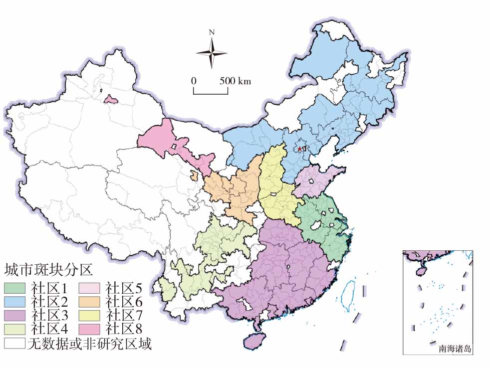
The results of semiconductor agglomeration area network partitioning with approximately maximized modularity
Fig.7
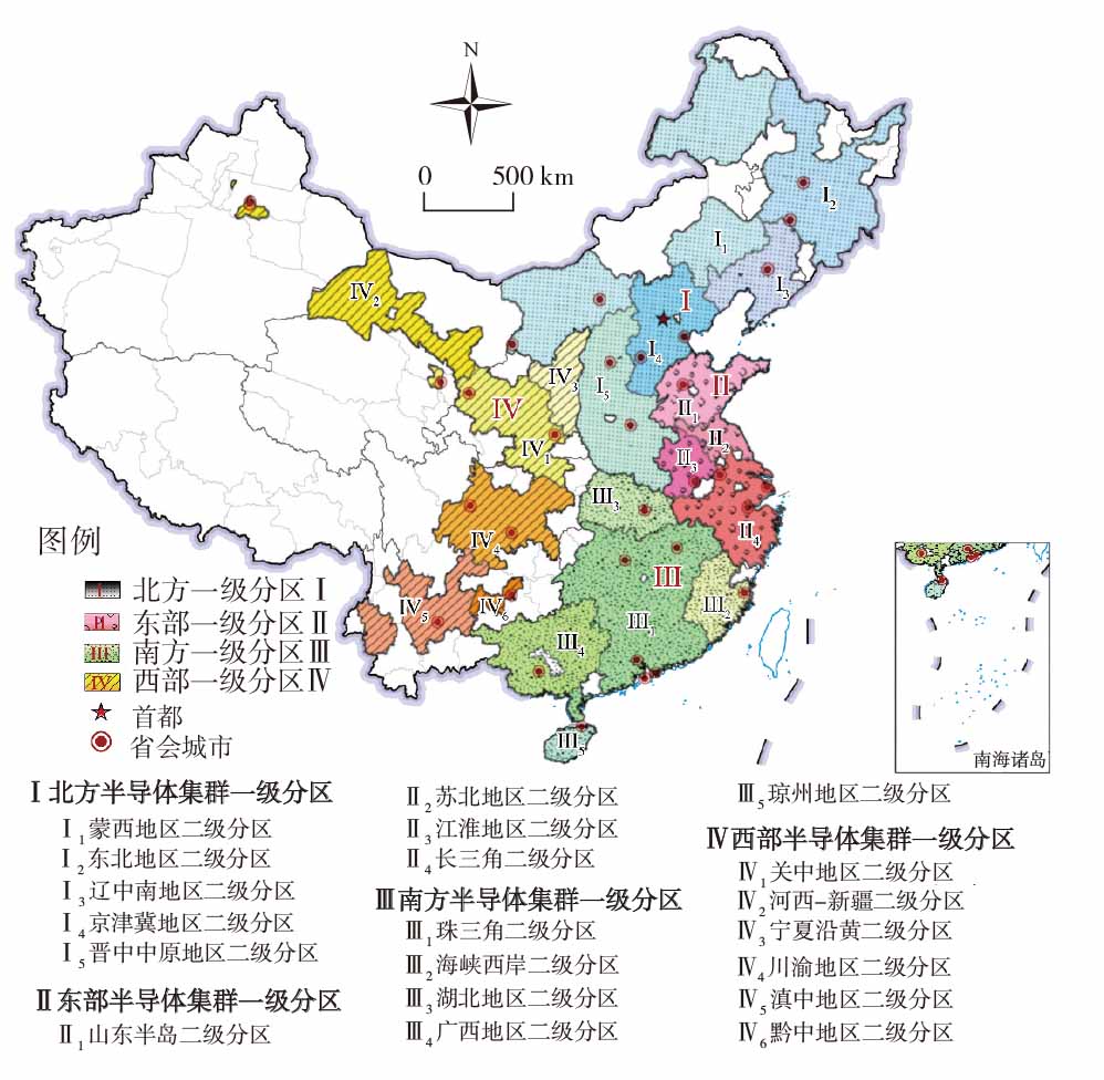
Second-level zoning scheme for the spatial agglomeration of China semiconductor industry
Tab.2
Indicators statistics of second-level zoning for the spatial agglomeration of the Chinese semiconductor industry